UPW Specifications for Semiconductor Cleanrooms
In our Semiconductor projects, ultrapure water is not a peripheral utility, but a critical process medium. Even traces of ions, organics, particles or dissolved gases can affect yield, oxide formation and the reliability of end products. That is why semiconductor-grade UPW is not just about “clean water”, but about tightly controlled specifications and stable quality right up to the point of use. Below, you can see which parameters matter, where UPW is used and which choices in water management and cleanroom delivery this entails.
Why even minimal contamination causes immediate process losses
Semiconductor processes are so sensitive that even minimal contamination can have a measurable effect, as discussed in Reducing particle deposition in wafer production. Ordinary tap water or standard purified water is therefore unsuitable: it can increase conductivity, leave residue or cause unwanted reactions. This translates into lower yield, altered oxide behaviour, corrosion and contamination of equipment parts and critical surfaces.
What semiconductor-grade UPW actually means
UPW is water in which virtually all non-H2O components have been removed, including ions, micro-organisms, organic compounds, particles and dissolved gases. Semiconductor-grade UPW goes far beyond standard purified or DI water. This quality is achieved through multi-stage water treatment and polishing, not through a single filtration step.
Which specifications determine whether UPW is truly usable in semiconductor applications
| Parameter | What you monitor | Which risk you limit |
|---|---|---|
| Resistivity / conductivity | Ionic purity and stability | Residue, leakage currents, process variation |
| TOC | Organic load | Films, deposits, chemical interference |
| Particles | Particulate contamination | Defects, scratches, yield loss |
| Micro-organisms | Biological load and biofilm formation | Contamination of loop and point of use |
| Dissolved oxygen | Oxidative load | Unwanted oxidation and corrosion |
The exact limit values depend on the process, tool and sensitivity. In practice, they are laid down in fab specifications, supplier criteria and industry roadmaps, with continuous monitoring alongside cleanroom control in accordance with ISO 14644-1, and in conjunction with the question: Which ISO or GMP class does your cleanroom need?
Where UPW is used in the cleanroom chain
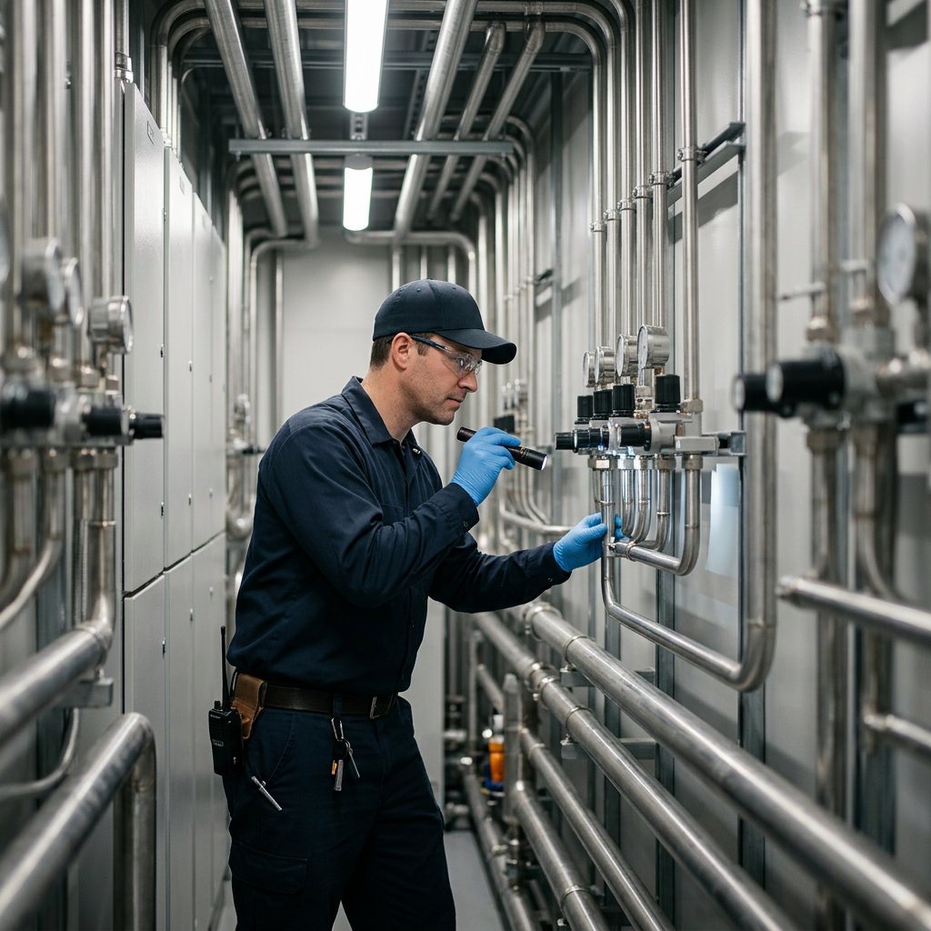
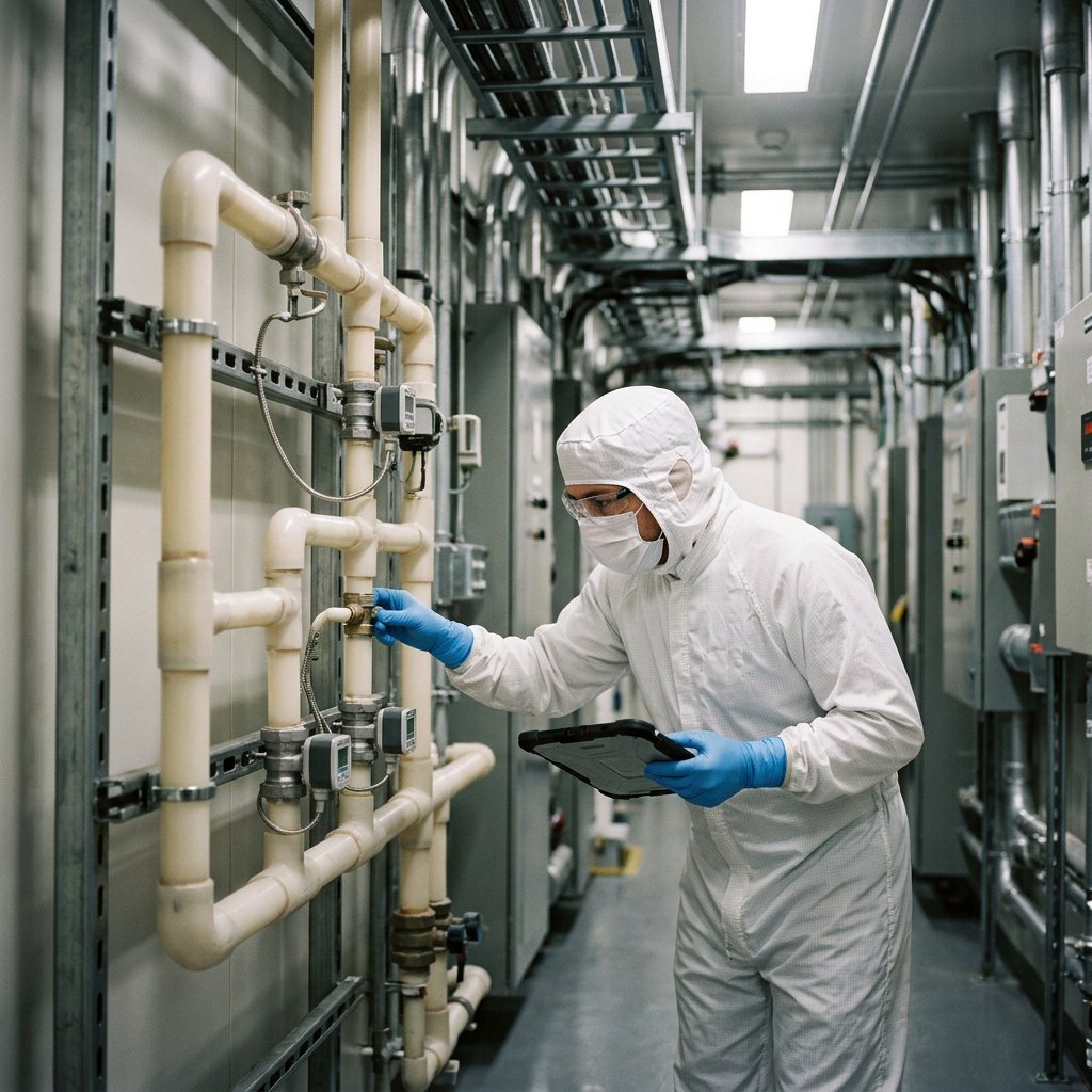
UPW is a critical process medium for cleaning, rinsing and keeping sensitive parts and surfaces clean. It therefore directly affects yield, reliability and the protection of equipment against contamination and corrosion. In cleanroom delivery, distribution, material selection, drainage and maintenance access must therefore support the required water quality right up to the point of use, as in the Nearfield Instruments cleanroom project.
High-pressure cleaning with UPW
In high-pressure cleaning, UPW is used through precisely selected nozzles to loosen films, residue and deposits. This can be a powerful cleaning method without additional chemicals and with limited risk of substrate damage. Its suitability does depend on the pressure setting, spray pattern and the sensitivity of the component being cleaned.
Hot DI or warm UPW for stubborn residues
Heating can weaken the bonds of contamination and helps remove organic or difficult-to-dissolve residues. Thanks to the lower surface tension, water also penetrates better into small openings and fine structures. This must be weighed against additional energy consumption, heat-up time and additional process configuration.
Water consumption, continuity and sustainability are part of the same UPW question
Chip fabs use a great deal of water, mainly because large volumes of UPW are needed for rinsing and cleaning steps. Water management is therefore not only about quality, but also about availability, recovery, redundancy and environmental impact. In cleanroom projects, capacity, storage, distribution and expandability must be defined early in the design, alongside environmental controls like Temperature stability for wafer metrology.
How we translate UPW requirements into semiconductor cleanrooms
At CSI, we align semiconductor and high-tech cleanrooms from the outset with utilities such as UPW. That translation into practice is reflected in routing, plant rooms, material transitions, drainage and maintenance access. With our modular wall and ceiling systems and the integrated Design - Engineer - Build - Care approach, we align process, construction and building services early on, so that expansion and maintenance remain possible with as little disruption as possible and contact with CSI about semiconductor cleanrooms can already take place in the design phase.