


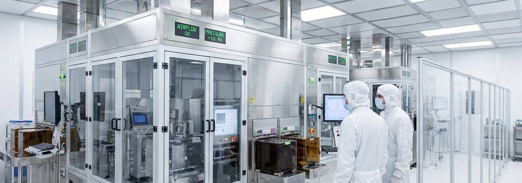
Semiconductor Cleanroom Design Criteria

A semiconductor cleanroom must control more than just dust particles. Stable chip production also depends on airborne molecular contamination (AMC), VOCs, electrostatic discharge, temperature, relative humidity, pressure differentials, airflow and vibration. That is exactly why not every process zone is assigned the same requirements: front-end steps such as lithography generally require stricter conditions than assembly, packaging or testing in the back-end process.
Table of Contents
- 1Why even a single particle can be too much in chip manufacturing
- 2Which ISO class fits which process?
- 3The design criteria that truly determine performance
- 3.1Particles, AMC and filtration
- 3.2Temperature, relative humidity and pressure hierarchy
- 3.3Airflow, FFU coverage and return air
- 3.4ESD, vibration and acoustics around critical tools
- 4How to determine the layout and zoning from front-end to back-end
- 5Standards, monitoring and validation should be defined early
- 6What determines the cost of a semiconductor cleanroom?
- Show more...
Key takeaways
- Control more than particles: include AMC/VOCs, ESD, temperature, RH, pressure, airflow and vibration.
- Select ISO classes per process zone and use local mini-environments for critical tools.
- Derive design values from process steps, tool sensitivity and yield targets to avoid under- and overspecification.
- Make airflow, FFU coverage, filtration and pressure cascades work as one coherent system.
- Define standards, monitoring and validation early; include commissioning, testing, calibration and FAT/SAT in scope.
The framework below helps you assess the right ISO or GMP class, zoning, technical boundary conditions and budget impact in practical terms. In doing so, themes such as class selection, validation, retrofit and modular construction connect logically, so you can see early on which design choices truly make the difference.
Why even a single particle can be too much in chip manufacturing
Semiconductor literally refers to a semi-conducting material and, in practice, to a component whose electrical properties are controlled with great precision. Because chips consist of extremely small structures and sensitive layers, even a minimal disturbance can already lead to process deviations.
A cleanroom environment is therefore not simply a clean room, but a controlled space in which particles, chemical contamination, climate, pressure, air distribution and electrostatic charge are actively controlled. This is necessary because contamination does not just cause visible defects. Yield loss, unstable process characteristics and later failures during inspection, packaging or test can also originate from an earlier deviation that was barely perceptible. Front-end wafer processes in particular are highly critical; back-end assembly and test environments remain controlled, but are usually less stringent than zones around lithography, etching or deposition.
Which ISO class fits which process?
Within ISO 14644, cleanroom classification runs from ISO 1 to ISO 9. In semiconductor manufacturing, a single class is rarely applied across the entire facility; in most cases you work with zone classes and, where necessary, even stricter local mini-environments around critical tools.
| Process zone | Usual ISO class range | Key design priorities |
|---|---|---|
| Lithography, resist processes and critical optical inspection | Often ISO 3 to 5 | Particle control, AMC/VOCs, lighting conditions, temperature stability and vibration control |
| Etching, deposition, implant, CMP, wet processes and metrology | Often ISO 4 to 6 | Stable airflow, chemical compatibility, pressure control and reliable filtration |
| Wafer handling, transfer zones, buffers and supporting front-end spaces | Often ISO 5 to 7 | Logistical separation, pressure hierarchy, transfer discipline and uniform air distribution |
| Back-end assembly, packaging and test | Often ISO 6 to 8 | ESD control, consistent cleanliness, controlled material flows and cost-efficient design |
These ranges are indicative. The definitive class depends on product risk, tool sensitivity, customer standards and the validation requirements you define in advance. In practice, a combination of room-based zone classes and locally stricter tool environments is often more efficient than designing an entire facility to one uniform, very high class.
The design criteria that truly determine performance
The performance of a semiconductor cleanroom results from a chain of choices that must align with one another. Filtration determines how many particles and how much molecular contamination are removed from the air, but without stable temperature, humidity, pressure control and a suitable airflow pattern, the process environment remains vulnerable. Add ESD control, vibration control and interaction with process equipment, and it becomes clear why a generic cleanroom concept is rarely sufficient in this sector.
The right design values are therefore not selected from a single standard template, but derived from the process steps, tool sensitivity and the desired yield. A lithography tool places different demands on air uniformity, vibration and AMC than a packaging line or test set-up. Gowning and access routes, material flows, maintenance access, utilities and the number of operators working simultaneously also affect final performance.
The tighter the tolerances, the greater the impact on design complexity, energy consumption and maintenance. More FFU coverage, finer filtration, more extensive monitoring and tighter control systems increase not only the investment, but also the service and calibration burden. That is exactly why early specification is important: it prevents underestimating risks in critical zones and over-specifying spaces where a lighter solution is technically sufficient. At CSI, that process logic is first translated into requirements, and only then into an appropriate modular construction and installation concept, as also reflected in semiconductor cleanroom projects.
Particles, AMC and filtration
Particles and AMC are different risks. Solid particles can settle on wafers, masks, optics or critical layers and thereby cause direct defects or pattern deviations, as in reducing particle deposition in wafer production. AMC concerns molecular contamination in the air, including organic components such as VOCs, acids, bases or other reactive substances that can affect surfaces, chemistry and measurement results.
For many cleanroom applications, HEPA filtration forms the basis. For finer semiconductor processes, ULPA filtration or additional AMC filtration may be required, depending on the process step and the sensitivity of the equipment. Yet a heavier filter package does not solve everything. Effective contamination control also starts with source control, material selection, correct zoning, pressure hierarchy and continuous measurement, so that deviations are detected early rather than only after yield loss.
Temperature, relative humidity and pressure hierarchy
Stable temperature and relative humidity limit process drift, reduce the risk of condensation and corrosion, and support a manageable ESD strategy. In semiconductor processes, even short fluctuations can affect critical steps or measurement results; in temperature stability for wafer metrology, that sensitivity is often directly visible.
That is why the pressure hierarchy between zones is also designed deliberately. With pressure steps, you direct the air from cleaner to less critical areas and prevent contamination from migrating the wrong way. Door frequency, interlocks, logistical routes and control systems must all support this; without proper monitoring, a theoretical pressure cascade quickly becomes unstable in practice.
Airflow, FFU coverage and return air
Not every semiconductor space requires the same airflow concept. Around highly critical steps, unidirectional downward airflow is often desirable to remove particles quickly and distribute the air uniformly across the work area. Less critical zones can sometimes be designed with a different distribution principle, provided the required class and process stability can demonstrably be achieved.
The required FFU coverage, the number of air changes, the ceiling configuration and the return concept are therefore directly related to process sensitivity. High coverage without good balance across all FFUs can still cause local deviations. The choice of return via plenum, low wall return or floor return also affects how effectively contamination is removed. The aim is always the same: to prevent turbulence, dead zones and recontamination, not simply to move as much air as possible.
ESD, vibration and acoustics around critical tools
ESD control in cleanrooms is not a stand-alone measure in a semiconductor cleanroom, but an integrated system. A conductive or dissipative floor, correct earthing, ionisation where required, suitable clothing and an appropriate humidity strategy work together to limit uncontrolled discharges. Especially with sensitive components or wafers, a small discharge can already cause damage that only becomes visible later.
Vibrations and acoustic disturbances play a major role particularly around lithography and other precision tools. Movement in the structure, fan imbalance or sound-driven microvibrations can have a direct effect on alignment, focus or reproducibility. That is why solutions such as decoupled structures, low-vibration motors and carefully balanced ventilation systems are applied mainly where the process risk truly justifies it. Here too, measuring and specifying before design prevents unnecessary costs afterwards. A concrete semiconductor case with advanced cleanliness and stability requirements is the Nearfield Instruments cleanroom project.
How to determine the layout and zoning from front-end to back-end
A good layout follows the process flow, not the other way round. This is illustrated in the Fonontech cleanroom.
- Base the room layout on process sequence, tool dimensions and critical transition zones, not solely on the existing building shell.
- Separate personnel, material and waste flows, and design pass-throughs, airlocks and service access before routing becomes constrained in practice.
- Reserve chase, subfab and other service areas early, so that maintenance and utilities disrupt the primary process as little as possible.
- Consider modular expansion or fit-out in an existing building only when the structure, utilities and contamination control demonstrably allow it.
Standards, monitoring and validation should be defined early
Anyone who only adds standards and validation at the end almost always creates avoidable remedial costs.
- Define the standards framework from the outset, with ISO 14644 as the basis and additional semiconductor, ESD or customer-specific requirements where relevant.
- Determine in advance which parameters will be continuously monitored and recorded, such as particles, AMC, temperature, RH, pressure differentials and airflow.
- Include commissioning, testing, calibration, FAT/SAT, certification and handover documentation in the project scope rather than only shortly before delivery.
- For more depth, this aligns with CSI knowledge on class selection, validation and positive-pressure or ventilation concepts, so that design and demonstrability remain aligned.
What determines the cost of a semiconductor cleanroom?
The price of a semiconductor cleanroom is rarely determined by floor area alone.
- The required class, process sensitivity, filtration stack, ESD measures, monitoring and the scope of validation are usually the main cost drivers.
- Per square metre, front-end zones are usually more expensive than back-end zones because of tighter tolerances and more demanding installations.
- Size, phasing, retrofit versus new build and a modular approach strongly influence investment, lead time and operational risk.
- Anyone who wants to estimate or compare can also find more detailed information at CSI about cleanroom costs, construction time and construction within an existing building.
Frequently asked questions
Related articles
Cleanroom interlock: operation, types and design considerations
A cleanroom interlock prevents…
Material Transfer in Aseptic Cleanrooms
Material and equipment transfe…
Cleanroom smoke study
A smoke study makes airflow vi…
